
No hay productos en la cesta.


Solving Power Adapter Noise: EMI Causes, Testing, and Compliance
We’ve all experienced it: a faint buzz from speakers when a charger is plugged in, static on an AM radio near a laptop, or unexpected glitches in sensitive equipment. This isn’t just an annoyance—it’s electromagnetic interference (EMI) from your power adapter, and it signals potential compliance issues and performance problems. As switching power supplies become faster and more efficient, managing their electrical noise has become both more critical and more challenging. This comprehensive guide demystifies EMI in external power supplies, exploring its root causes, how it’s measured, and the proven solutions that separate compliant, reliable products from problematic ones.
Chapter 1: Understanding EMI – The Invisible Culprit
What Exactly Is EMI?
Electromagnetic interference is unwanted electrical noise generated by electronic devices that can disrupt the operation of other equipment. For power adapters, this manifests as:
- Conducted EMI: Noise that travels along power cables (both input AC and output DC lines)
- Radiated EMI: Noise that propagates through the air as electromagnetic waves
The Real-World Impact:
- Audio systems: Hum, buzz, or whining through speakers
- Medical devices: Erroneous readings or malfunctions
- Wireless devices: Reduced range or connectivity drops
- Scientific instruments: Compromised measurement accuracy
- Regulatory consequences: Failed compliance tests preventing market entry
The Primary Sources in Switching Power Supplies
Switching regulators—the technology enabling compact, efficient adapters—are inherently noisy. The main culprits are:
1. The Switching MOSFET
- Rapid voltage transitions (dv/dt) during switching
- Creates high-frequency harmonics extending into the MHz range
- Visual Analogy: Like slamming a door repeatedly—each event creates a pressure wave (noise)
2. The Rectifier Diode
- Reverse recovery current spikes when switching off
- Generates ringing in the circuit due to parasitic inductance and capacitance
3. Parasitic Elements
- Trace inductance and transformer leakage inductance
- MOSFET output capacitance and diode junction capacitance
- These unintended components form resonant circuits that ring at high frequencies
4. Layout and Grounding Issues
- Improper component placement creating current loops
- Inadequate ground planes acting as antennas
- Shared return paths coupling noise between circuits
Chapter 2: The Root Causes – Why Your Adapter Makes Noise
Design-Level Causes
A. Switching Frequency and Its Harmonics
- Base frequency: Typically 50kHz to 500kHz in modern adapters
- Harmonic content: Noise extends to 30MHz (conducted) and 1GHz (radiated)
- Trend challenge: Higher frequencies improve size/efficiency but increase EMI challenges
B. Topology Choices
- Flyback converters: Most common, moderate EMI
- Forward converters: Better for higher power, different noise profile
- LLC resonant converters: Naturally lower EMI but more complex
C. Component Selection Pitfalls
- MOSFETs: Faster switching = more efficiency but sharper edges = more EMI
- Diodes: Standard silicon vs. Schottky (faster recovery)
- Capacitors: ESR/ESL characteristics affect filtering effectiveness
- Transformers: Inter-winding capacitance couples noise from primary to secondary
Implementation-Level Causes
D. Physical Layout Sins
- Long high-current traces: Act as radiating antennas
- Poor grounding: Creates ground bounce and common-mode noise
- Input/output proximity: Allows noise coupling between ports
- Heat sink placement: Can capacitively couple switching noise to chassis
E. Filtering Omissions and Compromises
- Undersized or missing input filters
- Improperly placed decoupling capacitors
- Absence of common-mode chokes where needed
- Cost-driven removal of “optional” filtering components
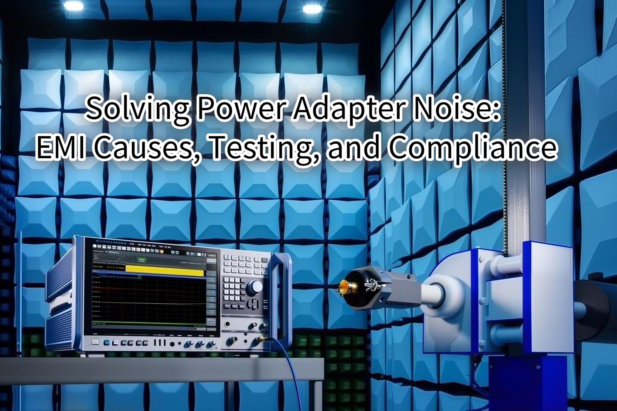
Chapter 3: Testing and Measurement – Quantifying the Problem
Regulatory Standards Framework
Global Requirements:
- FCC Part 15 (USA): Limits for digital devices
- CISPR 32 (International): Emission requirements for multimedia equipment
- EN 55032 (Europe): Harmonized with CISPR 32
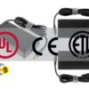
- Military/Medical: More stringent standards (MIL-STD-461, IEC 60601-1-2)
Key Limits for Power Supplies:
- Conducted EMI: 150kHz to 30MHz
- Radiated EMI: 30MHz to 1GHz (often extended to 6GHz)
- Class A vs. Class B: Commercial vs. residential environment limits
Testing Methodologies
1. Conducted Emissions Testing
- Setup: Line Impedance Stabilization Network (LISN) isolates adapter from lab power
- Measurement: Spectrum analyzer detects noise on both line and neutral conductors
- Typical failure points: Switching frequency harmonics, particularly 2nd and 3rd
2. Radiated Emissions Testing
- Setup: Anechoic chamber or open area test site
- Measurement: Antenna scans at multiple heights/orientations 3-10 meters from device
- Hot spots: Transformer regions, output cables, enclosure seams
3. Pre-Compliance Testing
- Budget-friendly approach: Using near-field probes and compact antennas
- Purpose: Identify issues before expensive full-compliance testing
- Tools: RF current probes, H-field/E-field probes, USB spectrum analyzers
The Testing Process: A Step-by-Step Overview
Design → Pre-compliance Testing → Identify Issues → Redesign → Formal Compliance Testing → Certification
Critical Insight: Each iteration at the compliance lab costs $2,000-$10,000, making pre-compliance screening essential.
Chapter 4: Proven Solutions and Mitigation Strategies
Level 1: Input Filtering Solutions
A. X-Capacitors (Line-to-Neutral)
- Purpose: Attenuate differential-mode noise
- Placement: Across AC input lines
- Typical values: 0.1μF to 1μF, safety-rated (X1 or X2 class)
B. Y-Capacitors (Line-to-Ground)
- Purpose: Attenuate common-mode noise
- Placement: From each line to earth ground or isolated secondary
- Critical constraint: Limited to 250μA leakage total (safety requirement)
- Typical values: 1nF to 4.7nF, safety-rated (Y1 or Y2 class)
C. Common-Mode Chokes
- How they work: High impedance to common-mode noise, low impedance to differential power
- Design considerations: Saturation current, frequency response, DC resistance
- Placement strategies: Multiple smaller chokes vs. one large choke
D. Integrated Filter Modules
- Combine X/Y capacitors and common-mode choke in one package
- Benefits: Simplified design, predictable performance, safety certification included
Level 2: Circuit Design Solutions
E. Switching Waveform Shaping
- Snubber networks: RC circuits across switching elements to damp ringing
- Gate resistors: Control MOSFET switching speed (trade-off: efficiency vs. EMI)
- Soft switching topologies: ZVS (Zero Voltage Switching), ZCS (Zero Current Switching)
F. Frequency Modulation Techniques
- Spread spectrum clocking: Dither switching frequency to spread energy
- Effect: Reduces peak emissions by 10-20dB
- Limitation: May not be acceptable in all applications (synchronization concerns)
G. Shielding and Isolation
- Transformer shielding: Faraday shield between primary and secondary windings
- Component shielding: Small cans over noisy components
- Board-level shielding: Copper fences or full enclosures
Level 3: Layout and Physical Design Solutions
H. PCB Layout Best Practices
- Keep high-current loops small: Minimizes radiating area
- Proper grounding strategy: Star ground for sensitive circuits, plane for digital
- Component placement: Filters close to noise sources, I/O connectors at perimeter
- Via usage: Multiple vias for low-impedance connections to ground planes
I. Enclosure and Mechanical Considerations
- Conductive coatings: On plastic enclosures for shielding
- Gaskets and seals: Maintain conductivity across seams
- Cable routing: Separate input and output cables, use ferrite beads if needed
- Aperture management: Keep holes smaller than λ/20 of highest frequency of concern
Solution Implementation Roadmap
| EMI Severity | Recommended Actions | Expected Cost Impact |
|---|---|---|
| Minor (Slight margin failure) | Optimize input filter values, Add output ferrite bead | 1-5% BOM increase |
| Moderate (Multiple dB over limit) | Add common-mode choke, Implement snubber circuits, Improve grounding | 5-15% BOM increase |
| Severe (Major redesign needed) | Change switching frequency, Add transformer shield, Implement spread spectrum | 15-30% BOM increase |
Chapter 5: The Compliance Process and Ongoing Management
Navigating Certification
- Pre-testing: Identify likely failure points using pre-compliance equipment
- Lab selection: Choose based on needed certifications (FCC, CE, etc.)
- Worst-case configuration testing: Vary line voltage, load conditions, cable positions
- Failure analysis: Correlate emissions peaks with circuit operation
- Mitigation implementation: Apply appropriate fixes based on failure characteristics
- Re-testing: Verify solutions don’t degrade other performance aspects
- Documentation: Prepare technical construction file (TCF) for regulatory submission
Maintaining Compliance in Production
The Quality Control Challenge: Component variations can turn a compliant design into a non-compliant product.
Strategies:
- Critical component control: Tight specifications on filter components
- Statistical testing: Sample-based testing in production
- Automated test equipment: Go/no-go testing for conducted emissions
- Process controls: Consistent assembly techniques (solder quality, shield connections)
Chapter 6: Case Studies – Practical EMI Solutions in Action
Case Study 1: The Noisy Laptop Adapter
Problem: A 65W adapter failing radiated emissions at 85MHz.
Investigation: Near-field probing identified the output cable as the radiating antenna.
Solution: Added a ferrite bead near the output connector and implemented a shield between primary and secondary transformer windings.
Result: 12dB improvement at 85MHz, passed Class B limits.
Case Study 2: Medical Power Supply Common-Mode Noise
Problem: Leakage current constraints limited Y-capacitor values, resulting in common-mode failures.
Investigation: Common-mode choke was saturating due to DC bias from unbalanced rectifier.
Solution: Implemented a balanced input circuit and used a choke with higher saturation current.
Result: Met both leakage current and emissions requirements.
Case Study 3: Cost-Driven Design Failure
Problem: A consumer adapter design removed “non-essential” filter components to save $0.35.
Consequence: 80% failure rate in production testing.
Solution: Restored two-stage input filter with optimized (not maximized) component values.
Cost Analysis: Added $0.28 to BOM but eliminated 100% rework/scrap costs.
Conclusion: Building Quiet Power from the Start
Solving power adapter EMI is not about applying band-aid fixes but implementing thoughtful design from the outset. The most successful approach follows this philosophy:
Design for EMI First:
- Start with the right topology for your power level and efficiency needs
- Incorporate filtering early in the schematic, not as an afterthought
- Plan the layout with EMI in mind before placing the first component
- Budget for proper filtering in your cost model—it’s not optional
- Test early and often with pre-compliance methods
The Compliance Mindset: EMI compliance shouldn’t be viewed as a barrier but as a quality marker. A quiet power supply is typically a well-engineered, reliable power supply. The discipline required to meet stringent EMI standards often results in better thermal performance, higher efficiency, and longer product life.
Final Recommendation: Whether you’re designing a million-unit consumer adapter or a specialty industrial supply, allocate engineering resources to understand your EMI profile. Invest in basic pre-compliance tools—they typically pay for themselves after avoiding just one failed compliance test. Remember that every decibel you reduce through good design is a decibel you won’t need to fight with filters later.
Resources and Next Steps
- Free Simulation Tools: Several PCB manufacturers offer EMI simulation with their design services
- Measurement Equipment Rentals: Affordable monthly rentals for spectrum analyzers and antennas
- Consulting Services: Many compliance labs offer design review services
- Continuing Education: IEEE and professional organizations regularly offer EMI/EMC courses
Dealing with a specific EMI challenge? Our technical team specializes in power supply design and troubleshooting. Contact us with your test results or design files for personalized recommendations.
Sobre el autor
Puestos relacionados

Choosing the right voltage for your power supply is a critical decision that affects performance, safety, and longevity of your electronic systems. While it may... Seguir leyendo

Power isn’t just an afterthought for your robot—it’s its lifeblood. Selecting the correct battery charger and power cord is one of the most critical, yet... Seguir leyendo

A high-performance CPU, a powerful GPU, fast storage—these are the components that capture our attention when building or upgrading a system. Yet, the component that... Seguir leyendo

In the vast landscape of industrial automation, we often celebrate the “brains” of the operation—the controllers and computers that make decisions. However, the true “muscle”... Seguir leyendo
 The Unsung Hero of Automation")
If you’ve ever wondered what keeps modern factories running smoothly, the answer is simple: Programmable Logic Controllers (PLCs) . These rugged industrial computers have been the foundation... Seguir leyendo


Añadir un comentario